Author Affiliations
Abstract
1 Tsinghua University, Department of Electronic Engineering, Beijing, China
2 Tsinghua University, International Center for Nano-Optoelectronics, Beijing, China
3 Arizona State University, School of Electrical, Computer, and Energy Engineering, Tempe, Arizona, United States
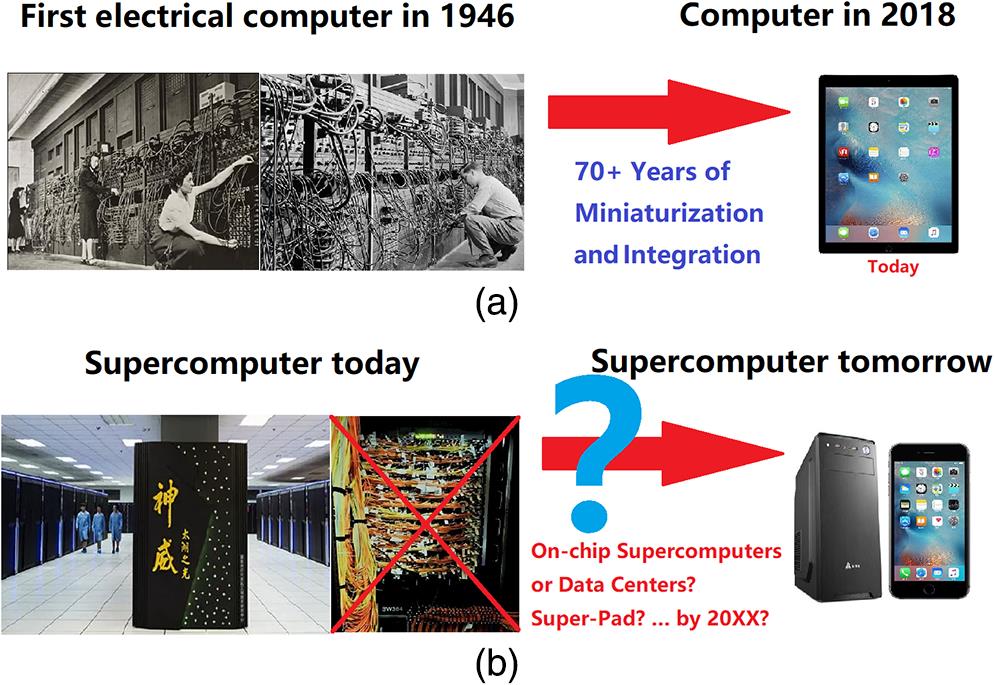
Semiconductor lasers, an important subfield of semiconductor photonics, have fundamentally changed many aspects of our lives and enabled many technologies since their creation in the 1960s. As in other semiconductor-based fields, such as microelectronics, miniaturization has been a constant theme, with nanolasers being an important frontier of research over the last decade. We review the progress, existing issues, and future prospects of nanolasers, especially in relation to their potential application in chip-scale optical interconnects. One of the important challenges in this application is minimizing the size and energy consumption of nanolasers. We begin with the application background of this challenge and then compare basic features of various semiconductor lasers. We present existing issues with nanolasers and discuss potential solutions to meet the size and energy-efficiency challenge. Our discussions cover a broad range of miniaturized lasers, including plasmonic nanolasers and lasers with two-dimensional monolayer gain materials, with focus on near-infrared wavelengths.
semiconductor lasers plasmonics photonic crystals two-dimensional monolayer materials energy efficiency optical interconnects Advanced Photonics
2019, 1(1): 014002
1 School of Electrical, Computer, and Energy Engineering, Arizona State University, Tempe, Arizona 85287, USA
2 Department of Electronic Engineering, Tsinghua University, Beijing 100084, China
Integrated photonics requires high gain optical materials in the telecom wavelength range for optical amplifiers and coherent light sources. Erbium (Er) containing materials are ideal candidates due to the 1.5 μm emission from Er3+ ions. However, the Er density in typical Er-doped materials is less than 1020 cm–3, thus limiting the maximum optical gain to a few dB/cm, too small to be useful for integrated photonic applications. Er compounds could potentially solve this problem since they contain much higher Er3+ density. So far the existing Er compounds suffer from short lifetime and strong upconversion effects, mainly due to poor crystal qualities. Recently, we explore a new Er compound: erbium chloride silicate (ECS, Er3(SiO4)2Cl) in the form of nanowire, which facilitates the growth of high quality single crystal with relatively large Er3+ density (1.62 × 1022 cm–3). Previous optical results show that the high crystal quality of ECS material leads to a long lifetime up to 1 ms. The Er lifetime-density product was found to be the largest among all the Er containing materials. Pump-probe experiments demonstrated a 644 dB/cm signal enhancement and 30 dB/cm net gain per unit length from a single ECS wire. As a result, such high-gain ECS nanowires can be potentially fabricated into ultra-compact lasers. Even though a single ECS nanowire naturally serves as good waveguide, additional feedback mechanism is needed to form an ultra-compact laser. In this work, we demonstrate the direct fabrication of 1D photonic crystal (PhC) air hole array structure on a single ECS nanowire using focused ion beam (FIB). Transmission measurement shows polarization-dependent stop-band behavior. For transverse electric (TE) polarization, we observed stop-band suppression as much as 12 dB with a 9 μm long airholed structure. Through numerical simulation, we showed that Q-factor as high as 11000 can be achieved at 1.53 μm for a 1D PhC micro-cavity on an ECS nanowire. Such a high Q cavity combined with the high material gain of ECS nanowires provides an attractive solution for ultra-compact lasers, an important goal of this research.
nanomaterials nanomaterials rare-earth-doped materials rare-earth-doped materials lasers lasers optical amplifiers optical amplifiers nanostructure fabrication nanostructure fabrication microcavity devices microcavity devices Frontiers of Optoelectronics
2016, 9(2): 312


